

Unbalanced Copper PCB
Boards with different copper weights across layers, built with controlled warpage.
Last updated
Unbalanced Copper PCB samples
-

4L BGA unbalanced copper board, 3.5/3 mil, immersion gold
-
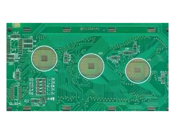
6L unbalanced copper PCB, 3/4 mil, solder bridge 0.1 mm
About Unbalanced Copper PCB
An unbalanced copper board has different copper weights or copper coverage on different layers, for example heavy copper on power layers next to thin copper for fine-pitch signal routing. Because copper and laminate expand at different rates, an unbalanced stack-up tends to bow and twist during lamination and reflow.
Keeping these boards flat takes careful stack-up planning and lamination control. We supply 4- and 6-layer unbalanced copper boards with BGA footprints, fine lines down to 3 mil and 0.1 mm solder mask bridges.
Typical applications
- Boards combining power and control circuits
- BGA boards with heavy power planes
- Motor drivers
- Power supplies
Common questions
How can I reduce warpage in an unbalanced design?
Keep the stack-up as symmetrical as the design allows, add copper fill to sparse layers, and avoid putting the heaviest copper on one outer side only. We can review your stack-up before fabrication.
How much bow and twist is acceptable?
IPC-6012 commonly allows 0.75% for boards with surface-mount components and 1.5% for other boards. Tell us if your assembly line needs a tighter limit.
Have a board to build?
Send us your Gerber files and requirements. Our team will review your specifications and get back to you with a quote.