
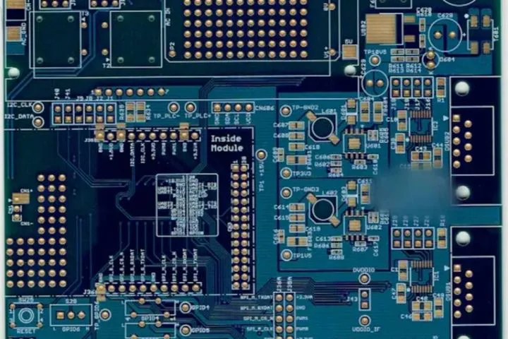
Printed Circuit Boards Rigid & flexible boards
Rigid, flexible and rigid-flex PCBs for prototyping and small-volume production, sourced from qualified partner factories and checked against your specifications.
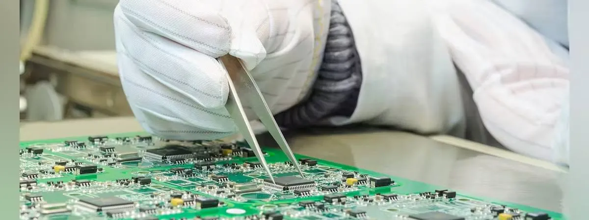
GL Circuits supplies PCBs from double-sided up to 40+ layers, with 3 mil (0.076 mm) minimum track and space, 4 mil laser-drilled holes and up to 10 oz copper, plus burn-in / HTRB / HAST boards and PCB design services.
Last updated
Our services
Printed circuit boards from prototype to small volume, reliability-test boards for semiconductor makers, and PCB design.
Rigid, flexible and rigid-flex PCBs for prototyping and small-volume production, sourced from qualified partner factories and checked against your specifications.
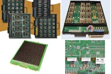
Fabrication and assembly of burn-in, high-temperature reverse bias (HTRB) and highly accelerated stress test (HAST) boards for semiconductor reliability testing.
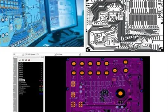
Design support that turns your schematics into board layouts ready for fabrication, so your project moves from concept to finished board with a single partner.
PCB capability
From double-sided boards to high-layer HDI with blind and buried vias, heavy copper and specialty laminates.
| Layer count | Double-sided to 40+ layers |
|---|---|
| Min. track width | 3 mil (0.076 mm) |
| Min. track spacing | 3 mil (0.076 mm) |
| Min. space track-to-pad, pad-to-pad | 3 mil (0.076 mm) |
| Min. drill hole diameter | 6 mil (0.15 mm) mechanical · 4 mil laser drill |
| Min. pad for vias | 12 mil (0.3 mm) |
| Max. PCB dimension | 23 × 35 in (584.2 × 889.0 mm) |
| PCB thickness | 8.27 – 275.8 mil (0.21 – 7.0 mm) |
| Max. copper weight | 10 oz |
| Solder mask bridge between solder dam | 4 mil (0.10 mm) |
| Min. solder mask annular | 1.5 mil (0.038 mm) |
| Plugged hole size | 0.15 – 0.5 mm |
| Surface treatment | HASL, gold plating, immersion gold, immersion tin, immersion silver, gold fingers (hard gold), OSP |
| Solder mask colors | Green, yellow, black, blue, matte, semi-matte, transparent LPI solder mask, peelable solder mask |
| Special materials | High-Tg FR4, high frequency (Rogers, Teflon, Arlon, Taconic), halogen-free, mixed-material lamination |
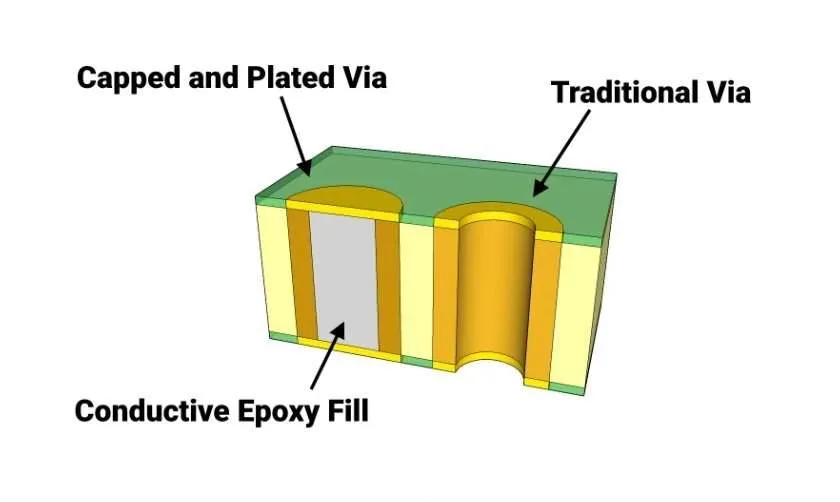
| Special techniques | Blind and buried vias (min. hole 0.1 mm), high layer count with heavy copper |
Values apply to 1 oz and 0.5 oz copper foil. For copper foil of 2 oz and above, the parameters change — send your stack-up for confirmation.
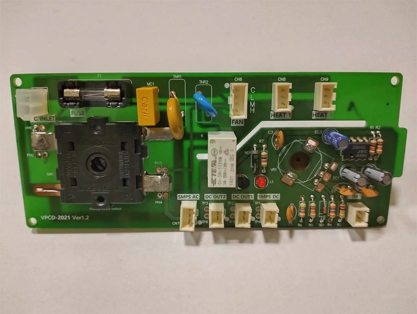
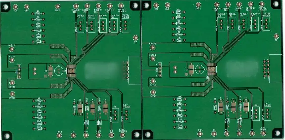
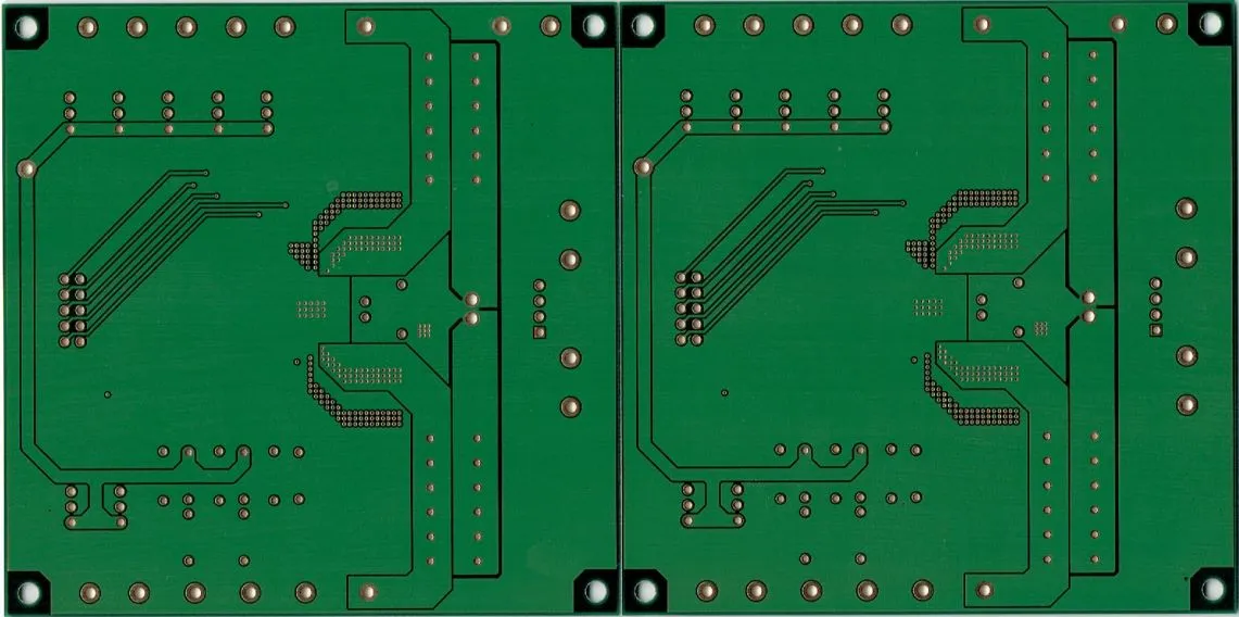
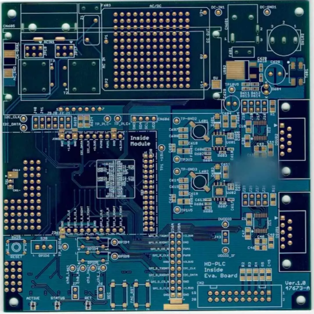
Gallery
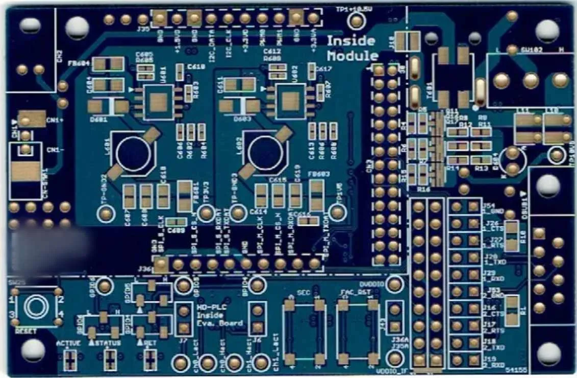
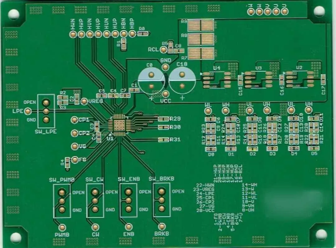
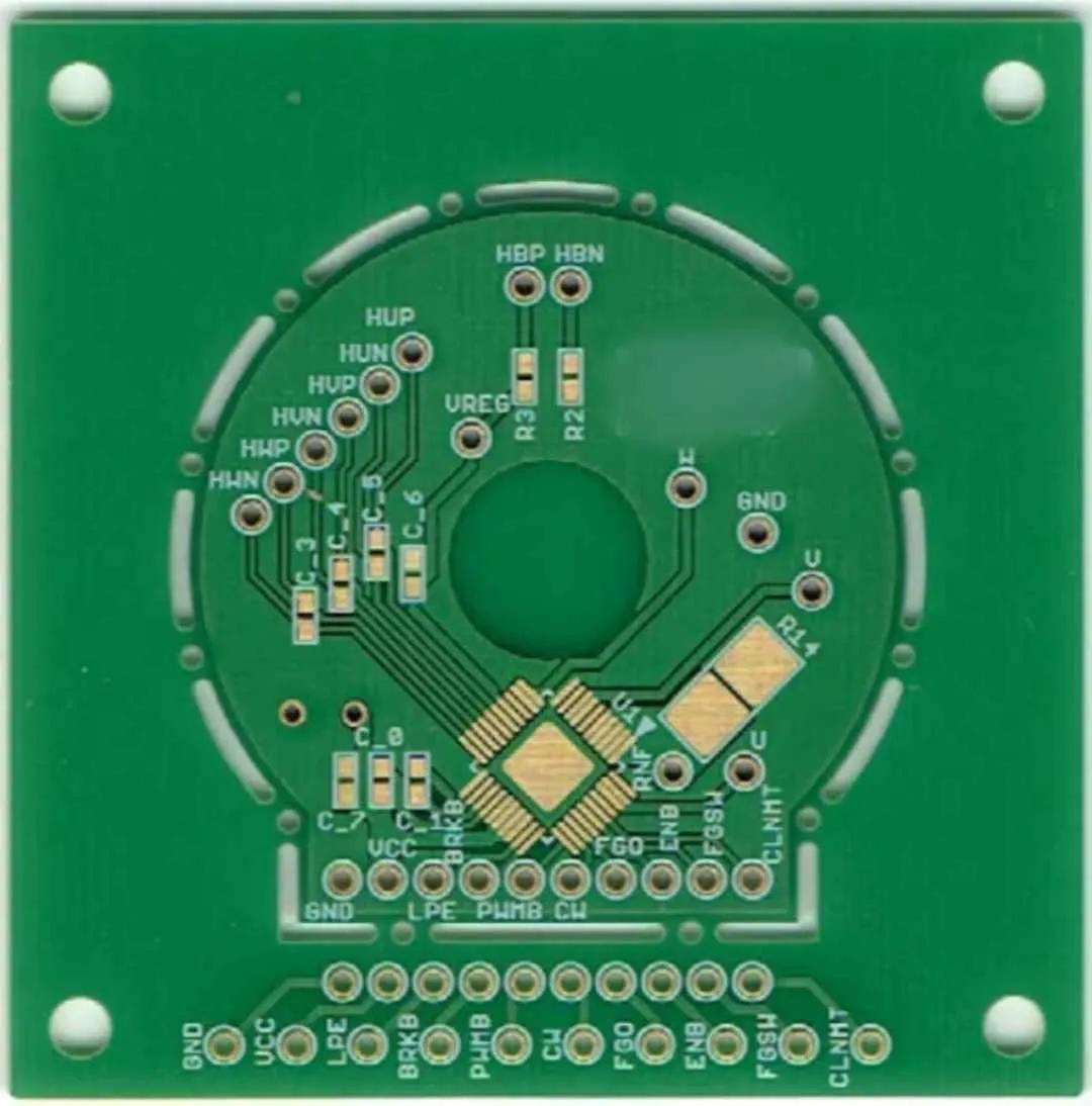
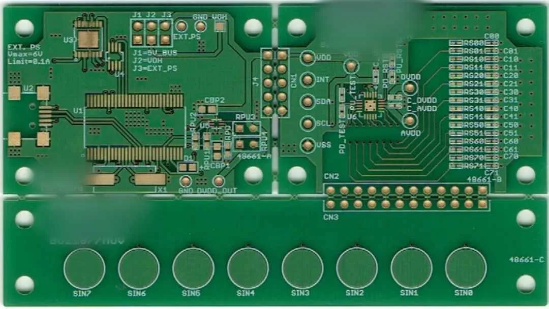
Select a photo to view it full size.
Send us your Gerber files and requirements. Our team will review your specifications and get back to you with a quote.